 Add My Company
Sign In

Electronic designs are constantly increasing in density and complexity. To deliver the end user experience the pressure is on component manufacturers to squeeze every ounce of performance from their devices. One result of this requirement is the selection of the correct voltage level to suit the application, which in turn has lead to the explosion in voltage rails that the PCB design has to accommodate on the PCB layout. The design of the PDN (Power Distribution Network) is critical to the overall performance of the finished product.
Traditionally, consideration of the PDN was not a major issue – power planes would be created for the major power supplies and local copper areas would be added to manage the lesser supplies. The designer would then use experience and rule of thumb to consider the implications. This solution is no longer adequate, some of the lesser supplies are increasingly very sensitive to any IR Drop because the voltage itself is so low to begin with; IR Drop and current density can no longer be treated in the traditional, rule of thumb, way.
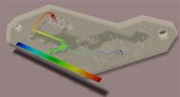
Through the use of the PDN Analyzer software, powered by CST®, we at TBS have the ability to analyse the physical copper at any stage during the design process to determine both the IR Drop and current density throughout the design. Using this analysis TBS can quickly and easily identify, assess and resolve any PDN issues during the design phase, giving the PCB designer the confidence that all the various will function correctly.
For more information on TBS Continue to Invest to Meet Today’s Design Challenges talk to Total Board Solutions Ltd
Enquire Now
List your company on FindTheNeedle.

