Sign In


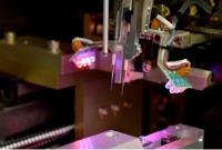
Flying probe testing has become an increasingly popular alternative to the more traditional in-circuit test for PCB assemblies.
One of the main benefits is that this method doesn't require a dedicated test fixture, which can save you both the initial expense and potential problems if the PCB changes or variants are required. Flying probes can also be programmed to probe almost anywhere, so space on the PCB for dedicated test pads isn’t a necessity either.
However, to get the very best from a flying probe test there are a few things that should be considered.
In this blog post, we take a look at 9 PCB assembly design guidelines we recommend you implement, in order to get the most from your PCB test strategy.
1. Handling
There needs to be a border edge, clear of components, along two opposite sides of the PCB so it can be held in the machine. Typically, this will need to be 3mm wide. Often the panel waste can be used, but if you are likely to need to test field returns, for example, then a clear edge needs to be included in the PCB design.
2. Fiducials
The machine needs these reference points to know where to place the probes. Again, these are often on the panel waste, but you should consider putting them on the PCB itself in case the waste has been removed.
3. Vias
It is possible and often convenient to probe on the edge of PCB vias, but to do this they must not be "tented"; this needs to be specified in the PCB design.
4. Component legs
If you want to probe near component legs, there needs to be space on the "toe" to probe. This is good practice anyway to achieve a good solder joint. Importantly, for test though, you don’t want to be probing on the component legs themselves, as any potential open circuit could be temporarily corrected at the point of test by the probe pressure pushing the component leg onto the pad.
5. Cleaning
The assembly, or at least the areas where you want to probe, need to be clean. This may mean removing any flux by cleaning the assembly, or ensuring that pin-probeable flux is used during production. If the tester has to repeatedly move its probe position to get better contact, test time can increase and false fails can occur.
6. Probe points
If possible, have accessible probe points for the ground and power rails on the bottom (perhaps unprobed) side of the PCB. This allows "fixed" probes - a bit like a temporary fixture - to be used for these points, which speeds up shorts testing and can much reduce the overall test time and cost.
7. Test access
Maximise test access on one side of the assembly if possible - i.e. have at least one probeable point for each network. Unless you’re using a double-sided machine, it costs more to turn the board over and test from both sides.
8. Component height
Consider component height on both sides of the PCB. There will be a maximum height allowed for both the probed and the underside of the PCB - typically around 40mm and 90mm respectively. Any tall components may have to go on the bottom side (if it is unprobed), or be fitted after test. It’s worth noting that tall components can also hinder test access, as they can create a "no fly" zone on the assembly.
9. Size
If you have a large PCB, try to keep the test access points as close together as possible. One of the drawbacks of flying probe test is that it is relatively slow, and much of the time taken is in moving the probes between measurement points.
Hopefully you have found this blog post of use and it has highlighted several points that you can build into your next design. By following these simple guidelines it’s entirely possible to reduce test times and costs while increasing coverage; making flying probe an even more viable alternative to in-circuit testing for smaller batches.
For more information on 9 PCB assembly design guidelines for Flying Probe test talk to ESCATEC Mechatronics Ltd
Enquire Now
More Blogs
List your company on FindTheNeedle.